- Joined
- Nov 21, 2020
I'm enjoying my time with KiCad for a project. Of course, if it was just designing a PCB that would be boring. I decided "hey, I want to make my own PCB" so I got a CNC router, finally re-built the electronics for it and now, many months later where I could have had 30 or 40 retries of PCBs made by a fab I'm almost ready to mill my own.
It's sort of fun figuring all this shit out. As you all know, "professional" PCBs are double sided and use something called "Plated Through Holes"(PTH) for connecting components. Which means for things like a Raspberry Pi Hat you can install the Pi connector facing down and all the other parts facing up. You can, of course, mill your own double sided PCB and even do PTH at home. The problem is doing copper plating is a pain in the ass, to get a thick enough layer you need to electroplate, which means the surface of the inside of a hole must already be conductive. There's various DIY solutions. One is to suck conductive ink through the holes and use that. Another involves electroless copper plating, but it's very thin. This requires a chemical that's nearly impossible for 'normal' people to get as it's also a drug making component. But there are now companies making kits, presumably with the naughty component mixed in so it can't be used. And they're expensive. Once the hole walls are activated by ink or plating then you do the electroplating with simpler chemicals like sulfuric acid. Another PTH option is little press-in eyelets, but they use a lot of space and for boards with connectors it might not work well.
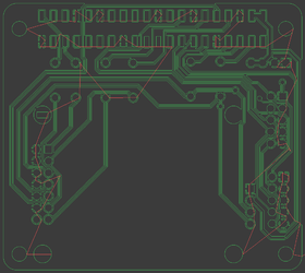
So, I took the lazy way out, a single sided board. But the connector for the Pi needs to be on the opposite side. So, the easiest way seems to be to make it a surface mount part and the rest of the stuff through-hole so they end up on the 'proper' side. The other thing single sided loses is "easy" ground planes since they're everywhere if you fill both sides and maybe just a couple vias to connect them. I ended up pushing traces around for quite a while to let the ground fill get as many spots as I could. Still ended up with 6 wire bridges, 2 for data and 4 to bring in a couple grounds I needed.
And the copper milling path might look something like this, maybe, thanks to pcb2gcode. There will also be a drilling holes file and a cut the edge out file.

Last edited:


